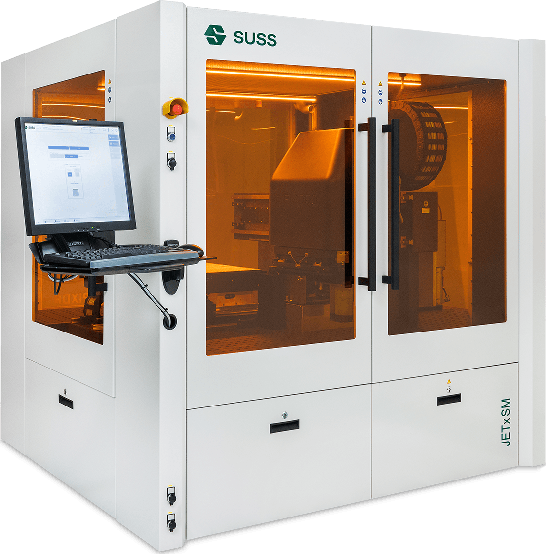
Go For Additive Solder Mask Manufacturing

Save time, material and production costs.

Only add material where it's required

That's what additive solder mask manufacturing is all about and that's what makes inkjet printing of solder mask so beneficial. Inkjet printing, being an additive process, means less process steps compared to traditional solder mask coating or Laser Direct Imaging (LDI). Photo and development process are eliminated as is the need for full surface flooding. This speeds up production while reducing waste, material and energy consumption.

Pre-treat
Inkjet Coat
Baking
Pre-treat
Coat
Expose LDI
Develop
Cure
Pre-treat
Coat
Produce Artwork
Expose
Develop
Cure

Inkjet Printing Process

How does it work?

Preparation

Outside of inkjet printing tool

  1. Surface pre-treatment of choice: Pumice or
    µEtch + Anti-tarnish
Solder mask coating

Using JETxSM

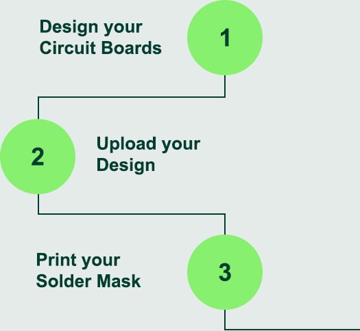
  1. Loading and board reading
  2. Alignment on 4 or more points
  3. Computation of image specific to board deformation and serialization
  4. Print
  5. UV Bump
  6. Unloading
Check out these six steps in this video
Post coating

Outside of inkjet printing tool

  1. Legend printing
  2. Baking: 60 min at 150 º C
  3. Metal finishing (HASL, ENIG, Sn/Ag immersion …)

SUSS JETxSM Inkjet Printer for PCB Solder Mask

SUSS JETxSM has the highest resolution on the market. One tool for rigid and flexible boards.

Design your printed circuit boards

Upload your design

Print your boards Opens up new design possiblities. Easier compliance with stricter future environmental regulation.

With JETxSM you can get started right away.

SUSS JETxSM with PiXDRO Technology
APEX Expo IPC 2019 Innovation Award Winner

JETxSM

The award winning novel inkjet-printed solder mask solution for PCBs enables drop-on-demand inkjet printing. The advantages of inkjet-based manufacturing are significant. It avoids costly photo processes, which typically include resist coating, exposure and development steps.

Inkjet Printing benefits

Why Inkjet Printing for PCB Solder Mask?

Additive and Cost-Effective
  • Solder mask is applied only where needed
  • Total costs of ownership lower than traditional technology
Digital
  • High resolution for pattern fidelity
  • Multi-fiducial marks alignment for astounding registration
Contactless
  • Insensitive to copper topography
  • Tolerates board height variations
Eco-friendly
  • Reduces chemical waste and material usage
  • Low energy consumption
Efficient
  • Precise production improves yield an increases productivity
  • Fast production speed for high throughput

JETxSM Features

Why SUSS JETxSM?

Accurately well-made, small and precise features

Small droplet size (2 pL)

High production speed

Bi-directional printing*

* Two UV LED arrays positioned on both sides of the print bar

High throughput

High jetting frequency and large number of nozzles (> 12.000)

Less maintenance and higher uptime

Unique ink recirculation always keeps the ink fresh and prevents air in the nozzles

“What you see is what you get” experience

Direct link of CAM software to print files in the inkjet system

Perfect layer coverage

Reliable solder mask thickness control at copper edges (4 µm and up)

High volume production

Printhead array with 6 parallel FUJIFILM Dimatix SambaTM G3L printheads

Boost Your PCB Manufacturing with JETxSM FE Software

How can JETxSM FE software improve additive manufacturing in solder mask application, even without operator skill and experience?

Take full advantage of additive manufacturing in solder mask application with the software package “JETxSM FE”. It bundles all necessary expertise on functional inkjet printing. Thus, printing jobs created by JETxSM FE provide the PCB manufacturer with supreme control on solder mask coating parameters like feature size and thickness. The JETxSM FE operates according to computer-aided manufacturing (CAM) principles, making its printing jobs directly available to the tool on the manufacturing floor. The specific printing job for each board is loaded and successfully printed. This ensures the best possible result even without specific operator skill and experience.

Solder Mask Manufacturing in Numbers

Some data why inkjet printing is amazing

Use of Ink
surface printed per kg of ink

up to 0
m2

Material savings
of up to

0
%

Number of Nozzles
up to

0

Number of drops per panel
up to

0

Watch JETxSM in Action

A close-up on details and a solder mask printed from beginning to end

The following videos, which have been released before the consolidation of the JETxSM name, will use previous names, such as "JETxSMP" or "JETx-M". The concepts and technologies that are depicted in the videos fully apply to the JETxSM.

Download Brochures

Brochure Solder Mask for PCB Brochure Jetx-M Product Information Brochure Inkjet Printing Technology

Contact our experts

You might be asking yourself …

  • Who can answer my questions about inkjet printing for PCB solder mask?
  • Who can fulfill my need for an in-depth discussion about the JETxSM Solder Mask tool?
  • When and how can I visit (virtually) the PrintLab for a live demo on the JETxSM Solder Mask tool?
  • How can I experience the difference between inkjet printing and traditional solder mask coating?

… And you want to read tech answer at your own pace, then
follow the “additive reality” column or watch a video Importance of Additive Manufacturing

… and you want to talk to us, then fill out below form: